Photonic Systems Group
University of California San Diego
RESEARCH
UC San Diego Photonic Systems Group has been involved in interdisciplinary research spanning nonlinear optics, fiber optical communications, sensing, silicon photonics and biophotonics. Most of the research is performed at the Photonic Systems Laboratory and the Micro/Nano-Fabrication Facility at the University of California San Diego, an environment where postdoctoral researchers, graduate and undergraduate students perform independent research. Still, many research projects are a part of large collaborative links with many universities and industry worldwide.
For more details about the ongoing projects, please use the menu on the left.
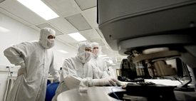
Nano3
Micro/Nano-Fabrication Facility
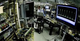
Photonic Systems Laboratory
Optical Measurement Facility
Much of the credit for the team's progress is attributed to the advanced facility located in the Atkinson Hall building. The 2,000-square-foot Photonic Systems Lab at Qualcomm Institute facility has a telecom-class space, supporting multicasting, synchronization, sampling, and system integration in one place, which has been fundamental in the achievements by the group. The laboratory closely emulates the Bell Laboratories model and has no equivalent in a university setting. The Photonic Systems Lab is modeled on the large, modular, industrial research labs where Professor Radic worked previously: Corning Research (1995-98) and Bell Labs (1998-2003).
The Nano3 facility in the Atkinson Hall building at UC San Diego provides advanced capabilities for fabrication and characterization in a state-of-the-art cleanroom and is one of 16 nation-wide sites of the National Science Foundation (NSF) supported National Nanotechnology Coordinated Infrastructure (NNCI). As a part of the Qualcomm Institute, the goal of Nano3 facility is to bring together interdisciplinary teams to facilitate research in electronics, optoelectronics, biomedical and biochemical devices, heterogeneous integrated devices and circuits, and sensor technology.